New Spin to an Old Conundrum: Measuring Surface Potential Faster (and better)!
An international team of scientists has developed a new approach to overcome time resolution in a popular scanning probe technique that can open pathways for real-time analysis of transient electronic and electrochemical properties.

Northern Ireland has a significant history in the field of electrostatics which forms the basis of modern-day electronics. Lord Kelvin, a native of Belfast and the first physicist to become a member of the House of Lords, made substantial contributions to this field. His famous quote, "If you cannot measure it, you cannot improve it," remains relevant to this day. One of Lord Kelvin's key contributions was the development of a technique for quantitatively assessing surface potentials. This technique, aptly named after him, has evolved into Kelvin Probe Force Microscopy (KPFM), which is widely used to measure surface potentials on the nanoscale with atomic force microscopes. Since its adoption in the early 1990s, KPFM has become a valuable tool in both commercial and research applications, allowing the study of material surface potentials, including metals, semiconductors, and biofilms. KPFM is particularly useful for understanding dynamic charge transport and the transient responses in nanoscale materials and devices. However, conventional KPFM has limitations in its time resolution due to spatio-temporal averaging.
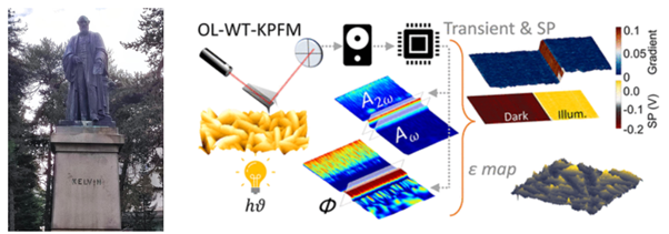
Conventional KPFM involves spatio-temporal (in space and time) averaging of probe-sample interaction which inherently limits its time resolution causing an irretrievable loss of transient response. To address this limitation, the team comprising of physicists and engineers at QUB, Ulster University, University of Dundee, Federation University (Australia) and Swinburne University (Australia) have led a collaborative effort and found a methodology capable of quantifying the sub-ms charge dynamics and probing the elusive transient response. The adapted KPFM technique can simultaneously extract spatial and temporal information from the photodetector signal to provide a dynamic mapping of surface potential, capacitance gradient, and dielectric constant at a temporal resolution three-orders higher than the conventional approach. The newly developed Open Loop-Wavelet Transform based KPFM has been employed to undertake mechanistic probing of surface potential changes arising from dynamic charge transport which can be key to understanding and engineering increasingly complex nanoscale materials and devices. The noteworthy work has been recently published in ACS Nano, a prestigious journal in the field of materials science, ranking among the top 2%.
Serene Pauly, a CDT-PIADS PhD student at QUB, led the experimental strand of the work undertaken at QUB and spent several sleepless nights finessing the experiments. She says, “The results are truly intriguing and demonstrate the method’s capability to address the limitations of conventional feedback based KPFM technique. We have already demonstrated that the novel approach can be used to explore the surface-photovoltage-induced sub-millisecond hole-diffusion transient in bismuth oxyhalide semiconductors. This feels like just a beginning though and the range of material systems where the approach can help unveil new material physics is expected to be large indeed.”
Dr Amit Kumar, Serene’s PhD supervisor and Head of CQMT (Centre for Quantum Materials and Technologies), added, “This work has been a true labour of love and could not have been possible without the strong collaboration between the engineers and physicists. The challenge lay in implementing the central idea on state-of-the-art scanning probe microscopes in our labs at QUB and UU. As we don’t use resonance-based feedback in our adapted approach to improve time resolution, we had to undertake significant denoising of the large data sets before extracting the local surface potential from them. After doing the hard yards to making the technique work well, we are truly excited at the opportunity to use the method in real-time analysis of transient electronic and electrochemical behaviour in materials going forward.”
